PCB Manufacturing
Engineering-Validated PCB Manufacturing for Real-World Production
What is a Printed Circuit Board(PCB)
A Printed Circuit Board, also known as a printed wiring board (PWB), is a fundamental component in nearly all modern electronic products. It serves as a laminated sandwich structure of conductive and insulating layers, designed to mechanically support and electrically connect electronic components. So the PCB’s quality and reliability are critical, as a defective PCB can be very expensive to rectify once components are mounted.
PCB Manufacturing Built for Manufacturability and Reliability
We fabricate PCBs with a production-first mindset
ensuring your boards are ready for assembly, reliability, and scaling.
As your production team in China, we don’t treat PCB fabrication as a standalone step,
But as the foundation of your entire manufacturing process. Every board we produce is reviewed, validated, and prepared for real-world assembly and volume production—reducing downstream risk before it becomes costly.
About
Our PCB Manufacturing Features
Built for Assembly, Reliability, and Scale
Engineering-Reviewed Before Fabrication
We don’t fabricate directly from files.
Every PCB goes through DFM and production feasibility review to identify layout, stack-up, and material risks before manufacturing begins.
Assembly-Oriented Stack-Up & Material Selection
PCB materials and stack-ups are validated based on real assembly and operating conditions, not just electrical specs, which will improve soldering yield, stability, and long-term reliability.
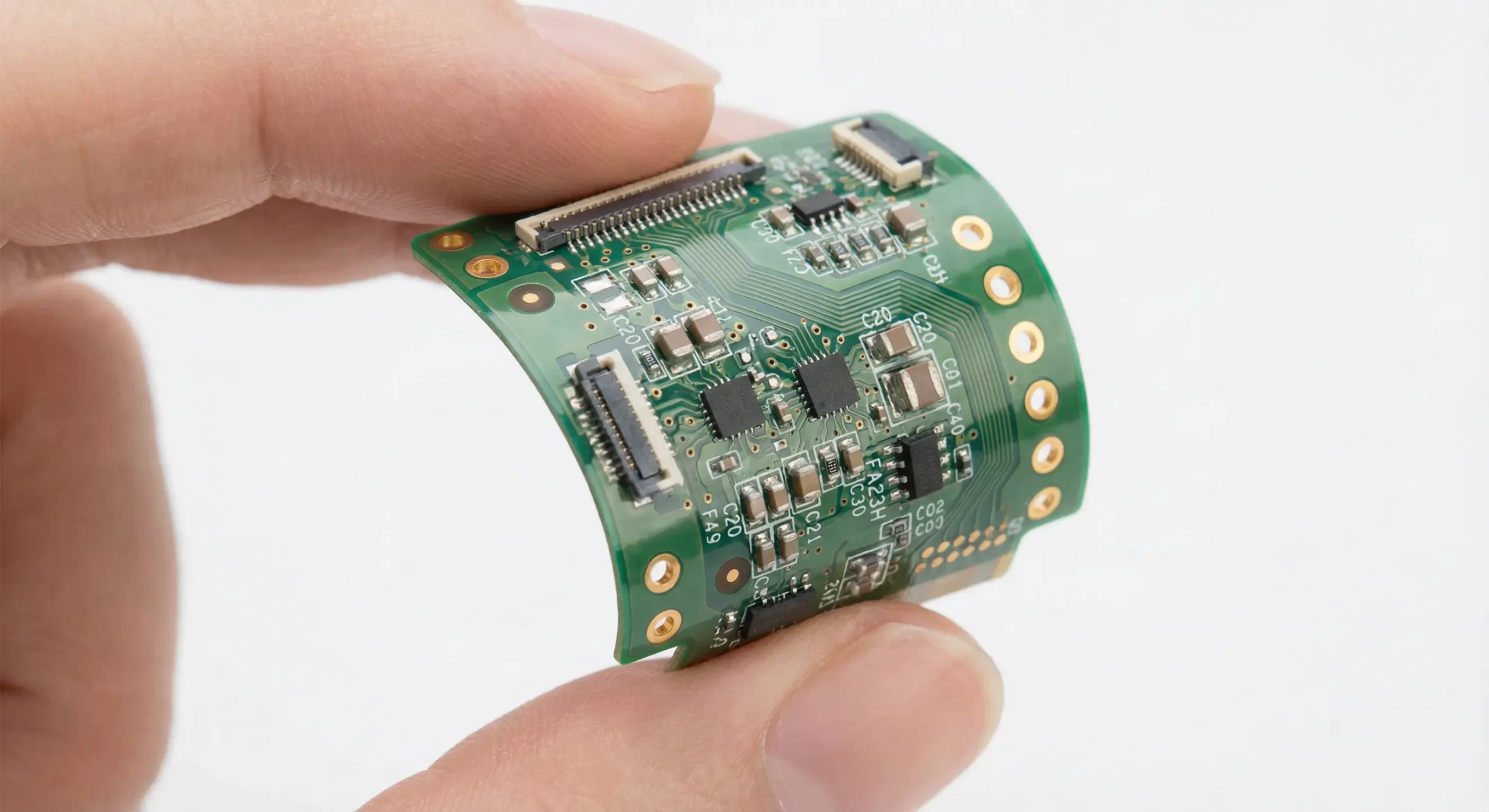
Flexible Technology Coverage
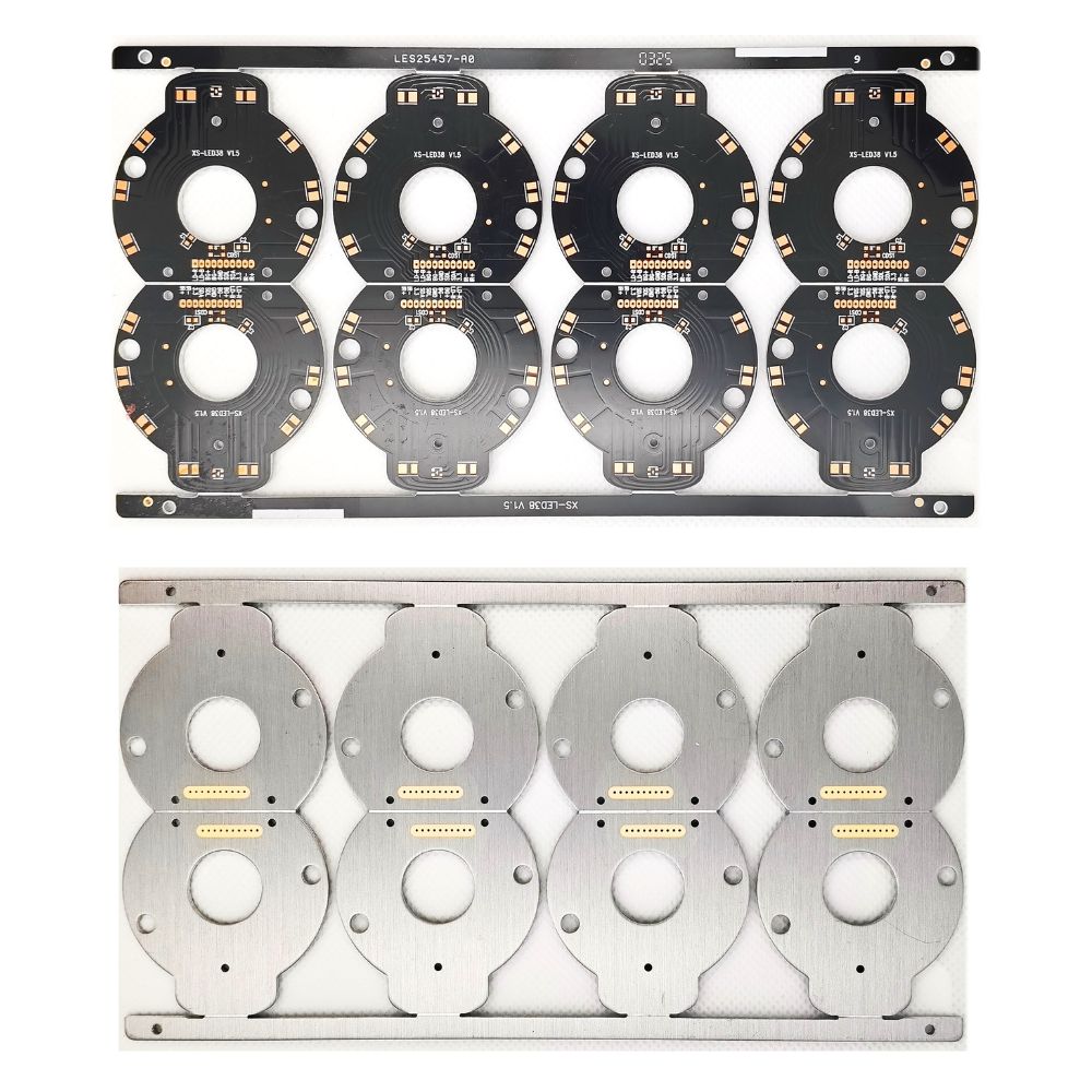
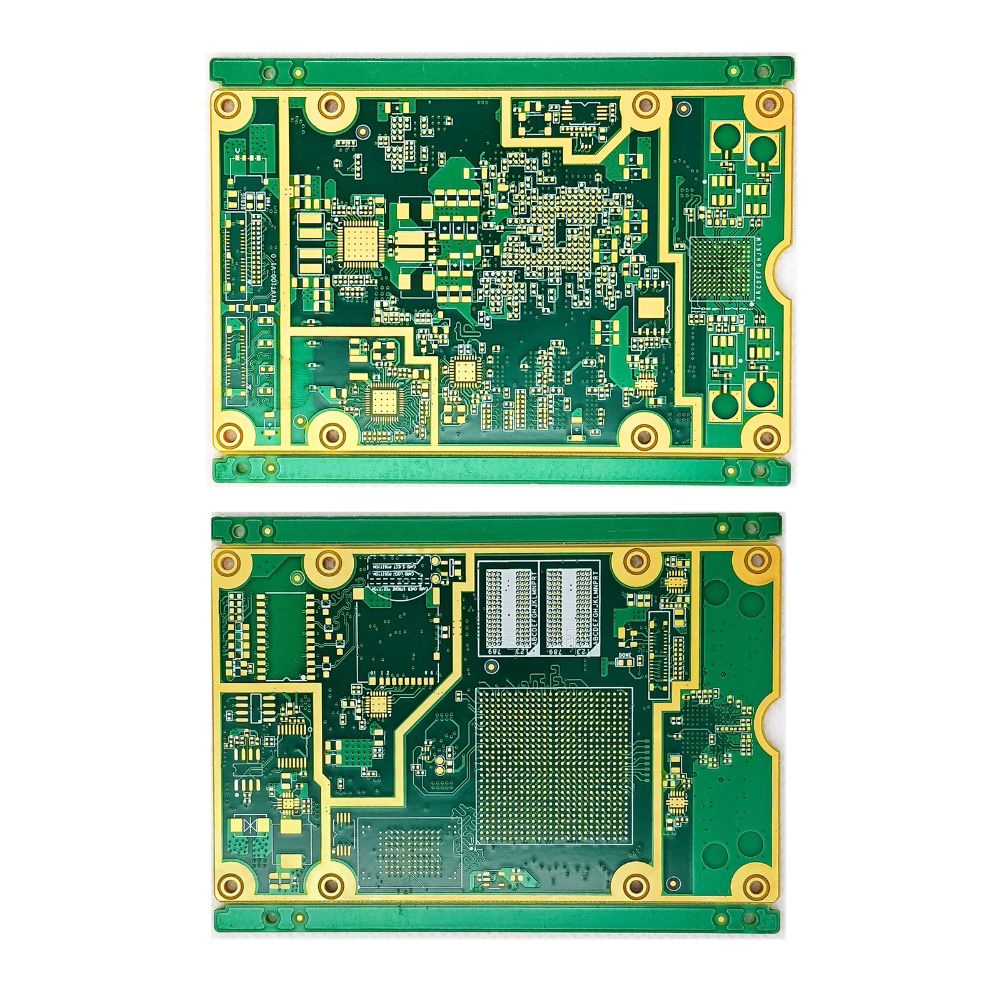
From simple boards to complex designs, we support a wide range of PCB types from Rigid to Flex-Rigid PCBs, HDI, and Multilayer boards. controlled impedance design to meet your production needs,
Tight Integration with PCBA & Turnkey Builds
PCB manufacturing is fully aligned with our Turnkey PCB Assembly and Box Build processes. So the issues are identified at the PCB stage—not after components are already mounted.
Traceability & Process Control
We enforce material traceability, process documentation, and controlled manufacturing flows across our PCB manufacturing. It provides consistent quality, audit readiness, and confidence when scaling production.
Manufacturing for Change, Not Just Stability
We are used to frequent design updates, fast revisions, and compressed schedules, especially in IoT and engineering-driven projects. The design changes won’t derail your production plan.
The Challenges & Approach
The Problem We See Too Often
Many PCB issues don’t come from fabrication errors —
They come from designs that were never validated for production reality.
- Redesigns are triggered only after PCBA or pilot builds
- PCBs that pass fabrication but fail during assembly
- Stack-up or impedance mismatches discovered too late
- Material selections that cause yield loss or reliability issues
Once the boards are fabricated with components mounted, many problems become expensive or impossible to fix.
Our PCB Manufacturing Approach
Helptron approaches PCB manufacturing as part of a complete production system, not a separate vendor process or standalone step.
- Design-for-manufacturability (DFM) review
- Stack-up and impedance validation
- Material selection aligned with assembly and reliability requirements
- Risk identification for downstream PCBA and box build
This ensures your PCB is not only manufacturable, but production-ready.
Why Engineering-validated PCB manufacturing Matters?
Early PCB decisions directly impact the success of the entire product.
Engineering-validated PCB manufacturing helps you:
- Improve yield and reliability at scale
- Prevent costly PCBA scrap
- Reduce first-build failures
- Avoid late-stage redesigns
- Shorten overall project timelines
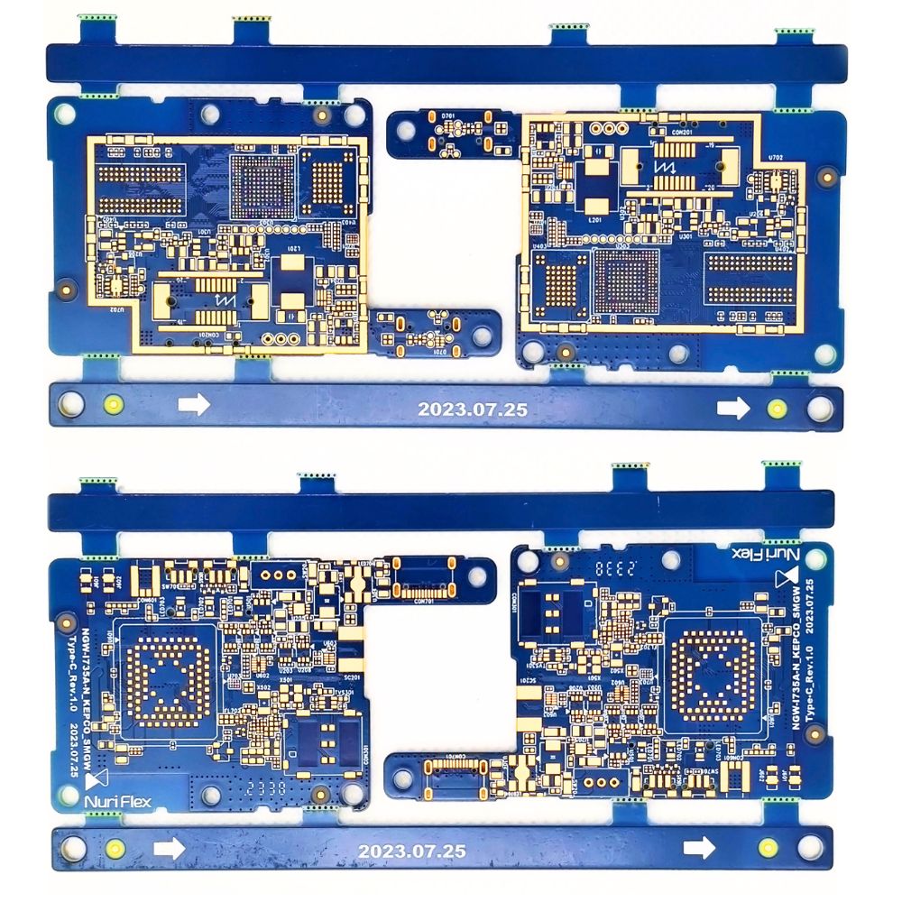
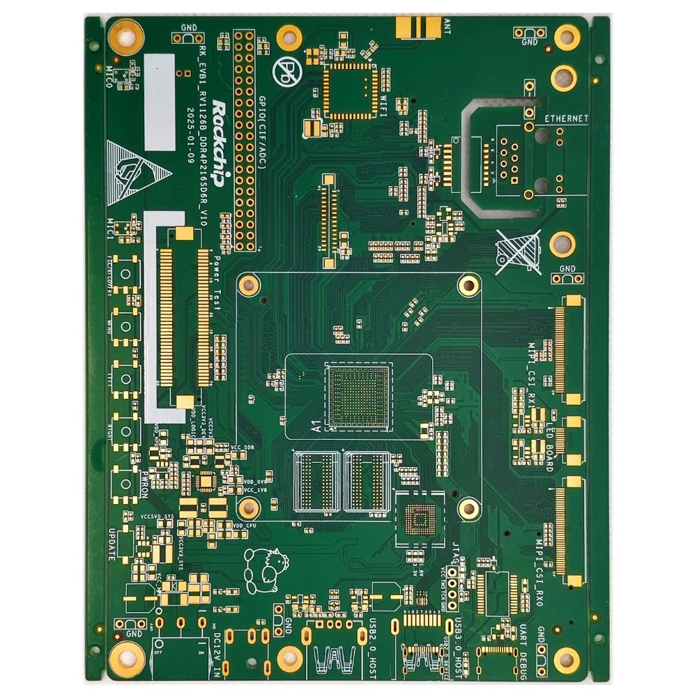
PCBs We Offer
By Types
- Rigid PCB
- Flexible PCB
- Rigid flexible PCB
- Blind viasion, buried vias
- Via In Pad, including VIPPO
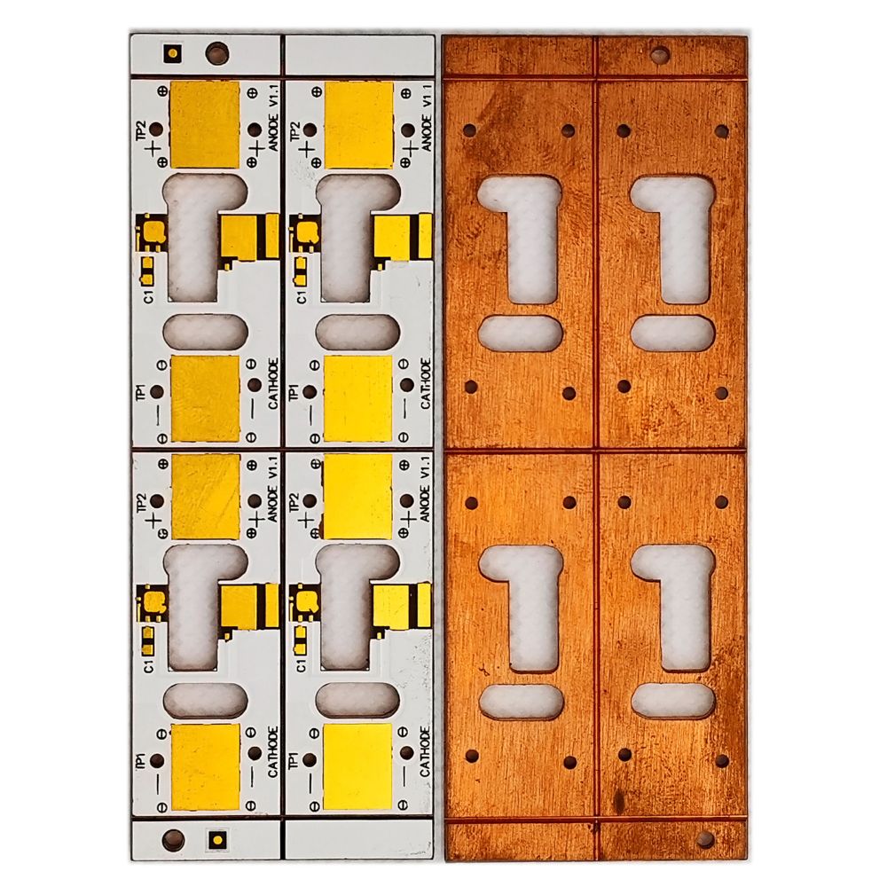
- Aluminum base PCB
- Copper base PCB
- RF Microwave
- High frequency
- High speed
- Impedance Control
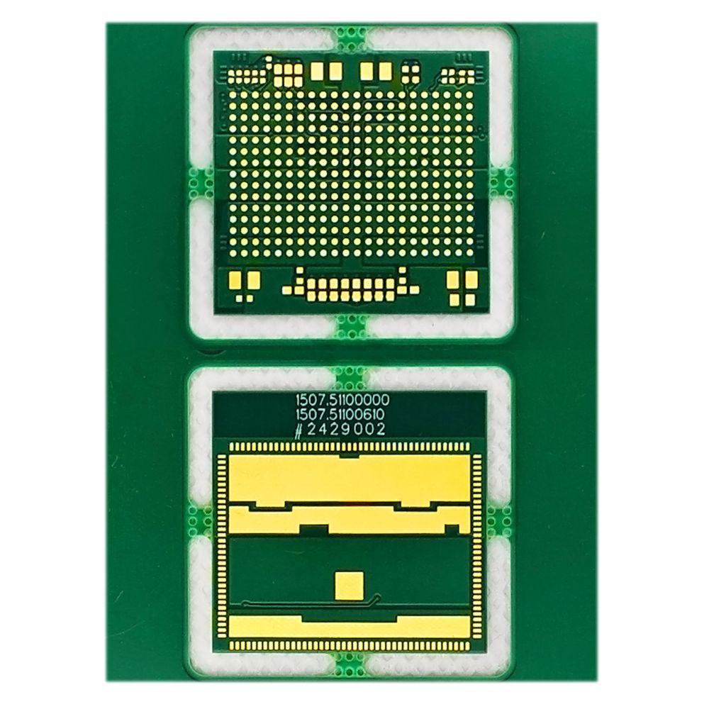
- PCBs with IC Substrate
- Backplane, back drill
By Material
- FR4 PCB
- Rogers PCB
- Ceramic PCB
- Polyamide PCB
- Semiflex PCB
- Isola PCB
- Teflon PCB
- Alumina PCB
- High Tg PCB
- Halogen Free PCB
- Copper Based PCB
- Taconic PCB
- Low Loss PCB
By Features
- Heavy Copper PCB
- Blind and Buried Vias
- Microvia PCB
- VIPPO PCB
- High-Frequency PCB
- High Speed PCB
- Quick Turn PCB
- Single-Sided PCB
- Double Sided PCB
- 4 Layer PCB
- 6 Layer PCB
- IC Substrate PCB
- Embedded PCB
By Markets
- Power PCB
- Led PCB
- Inverter PCB
- Control PCB
- Sensor PCB
- Amplifier PCB
- Radar PCB
- Medical PCB
- Automotive PCB
- Capacitive PCB
- HVAC Circuit Board
- UPS Circuit Board
- Industrial PCB
Manufacturing Capabilities
We specialize in rapid PCB manufacturing, offering 24- or 48-hour turnaround options to keep your project moving. From IoT startups to industrial device makers, our customers count on us for precision, speed, and flexibility. Whether you need one prototype or thousands of production units, Helptron delivers high-quality PCBs — on time and on budget.
| Item | Standard | Limitation |
|---|---|---|
| Material | CEM-1/CEM-3/FR4 | High Frequency Series / High Tg |
| Layers | 2-14layers | 18Layers |
| Max Size | 580x620mm | 580x900mm |
| Finished Thickness | 0.4mm to 3.5mm | 0.3mm to 5.4mm |
| Copper Weight | 1/2oz to 3oz | 5oz |
| Wrapage | 0.75% (Max) | 0.5% |
| Impedance Tolerance | Natural Impedance +/- 10% DIfferential Impedance +/- 10% | Natural Impedance +/- 8% DIfferential Impedance +/- 8% |
| Surface Finished | LF HASL ENIG OSP Immersion Tin | Hybrid Surface Treatment |
| Line Width/Space | > 1/2oz 3mil/3mil >1oz 5mil/5mil >2oz 7mil/7mil >3oz 9mil/9mil >4oz 11mil/11mil | > 1/2oz 2.5mil/2.5mil >1oz 4mil/4mil >2oz 5mil/5mil >3oz 8mil/8mil >4oz 10mil/10mil |
| Min Hole Diameter | 0.2mm | 0.15mm |
| Max Hole Diameter | 6.5mm | N/A |
| Hole Copper Thickness | 12um To 25um | Max 50um |
| Solder Mask | Green / Black / White / Blue / Red | Yellow /Coffee |
| Solder Mask Thickness | Line/copper surface 12um to 25um Line Angle 5um To 15um Base material position 18um to 35um | 10um To 28um 10um To 26um 35um |
| Min Solder Mask Bridge | Base Copper Thickness<H/Hoz, 2.5mil Base Copper Thickness<1/1oz, 3.5mil Base Copper Thickness <2/2oz, 1mil Base Copper Thickness <3/3oz, 5 mil | N/A |
| Overlay | Min width: 10mil Min Height: 30mil Min Overlay S/M Bridge: 6mil | N/A |
| Carbon Ink | Min Width: 14mil | 12mil |
| Lead Free HASL Thickness | 0.8um To 40um | 2.5um To 40um |
| ENIG Thickness | Nickel : 2.54um< Max<5um Gold: 0.025um<Max<0.05um | N/A |
| V-Cut Slot | Board Thickness:0.4mm< Max<3.0mm | 0.2mm<Max<5.0mm |
| Package | EPE Foam and Vacuum Packing | N/A |
Consult with Special Specifications If The Table Below Can not Meet Your Specified Requirements.
PCB Manufacturing FAQs
Do you review our PCB design before fabrication?
Yes. Every PCB project is reviewed by our manufacturing engineers before fabrication.
We check stack-up, materials, tolerances, and potential assembly risks to ensure the design is manufacturable and aligned with downstream PCBA requirements
Can you support prototype and low-volume PCB builds?
Absolutely. We specialize in prototype, NPI, and low-to-mid volume PCB fabrication.
Our processes are designed to support evolving designs without forcing volume-driven constraints
How do you ensure PCB fabrication aligns with PCBA and assembly?
PCB fabrication at Helptron FPC is planned together with PCBA and assembly requirements.
Board specifications, surface finish, and tolerances are confirmed based on actual assembly and test processes — not treated as an isolated step.
What PCB materials and surface finishes do you support?
We support standard and high-Tg FR-4 materials, as well as selected specialty laminates when required.
Common surface finishes include ENIG, OSP, and HASL, selected based on product reliability and assembly needs.
How do you handle controlled impedance and tight tolerances?
Controlled impedance and tolerance requirements are reviewed and validated during the engineering review stage.
We coordinate fabrication parameters with PCBA requirements to ensure electrical and mechanical consistency.
What quality controls are in place during PCB manufacturing?
Quality control includes material verification, in-process inspection, and electrical testing where required.
In addition, fabrication data is cross-checked against assembly needs to prevent downstream issues.
Can you help identify potential manufacturing risks early?
Yes. Early risk identification is a core part of our approach.
By reviewing PCB design and fabrication choices before production, we help prevent yield loss, rework, and delays during assembly.
How do you manage design changes or revisions?
We support design iterations common in NPI and early production stages.
Revisions are reviewed by engineering to ensure changes do not introduce new fabrication or assembly risks.
Do you fabricate PCBs as a standalone service or as part of full EMS?
Both. However, PCB manufacturing delivers the most value when integrated with our PCBA and EMS services, where fabrication decisions are optimized for the full production lifecycle.
Why not source PCBs separately to reduce cost?
Separating PCB sourcing may reduce unit cost on paper, but often increases total project risk and hidden costs.
By managing PCB fabrication as part of an integrated manufacturing process, we help reduce rework, delays, and overall production risk.